- 您现在的位置:买卖IC网 > Sheet目录345 > MT42L256M32D4KP-3 IT:A (Micron Technology Inc)IC LPDDR2 SDRAM 8GBIT 168FBGA
�� �
�
�2Gb:� x16,� x32� Mobile� LPDDR2� SDRAM� S4�
�Burst� READ� Command�
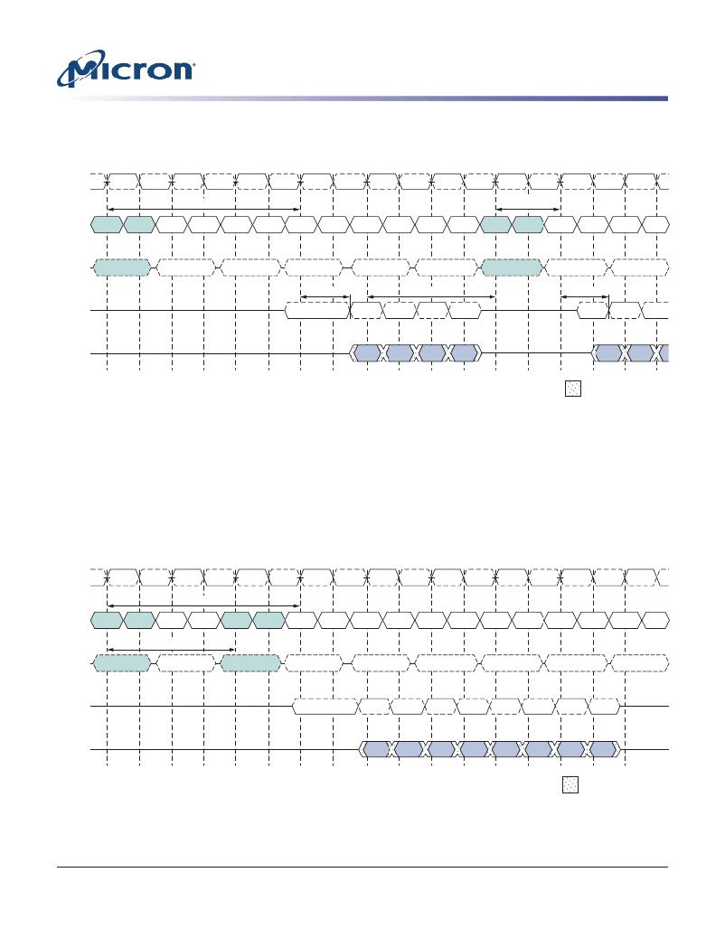
�Figure� 36:� Burst� READ� Followed� by� Burst� WRITE� –� RL� =� 3,� WL� =� 1,� BL� =� 4�
�T0�
�T1�
�T2�
�T3�
�T4�
�T5�
�T6�
�T7�
�T8�
�CK#�
�CK�
�RL� =� 3�
�WL� =� 1�
�CA[9:0]�
�Bank� n�
�col� addr�
�Col� addr�
�Bank� n�
�col� addr�
�Col� addr�
�CMD�
�READ�
�NOP�
�NOP�
�NOP�
�NOP�
�NOP�
�WRITE�
�NOP�
�NOP�
�DQS#�
�DQS�
�t� DQSCK�
�BL/2�
�t� DQSSmin�
�DQ�
�D� OUT� A0�
�D� OUT� A1�
�D� OUT� A2�
�D� OUT� A3�
�D� IN� A0�
�D� IN� A1�
�D�
�Transitioning� data�
�The� minimum� time� from� the� burst� READ� command� to� the� burst� WRITE� command� is�
�defined� by� the� read� latency� (RL)� and� the� burst� length� (BL).� Minimum� READ-to-WRITE�
�latency� is� RL� +� RU(� t� DQSCK(MAX)/� t� CK)� +� BL/2� +� 1� -� WL� clock� cycles.� Note� that� if� a� READ�
�burst� is� truncated� with� a� burst� TERMINATE� (BST)� command,� the� effective� burst� length�
�of� the� truncated� READ� burst� should� be� used� for� BL� when� calculating� the� minimum�
�READ-to-WRITE� delay.�
�Figure� 37:� Seamless� Burst� READ� –� RL� =� 3,� BL� =� 4,� t� CCD� =� 2�
�T0�
�T1�
�T2�
�T3�
�T4�
�T5�
�T6�
�T7�
�T8�
�CK#�
�CK�
�RL� =� 3�
�CA[9:0]�
�Bank� n�
�col� addr� a�
�Col� addr� a�
�Bank� n�
�col� addr� b�
�Col� addr� b�
�t� CCD�
�=2�
�CMD�
�READ�
�NOP�
�READ�
�NOP�
�NOP�
�NOP�
�NOP�
�NOP�
�NOP�
�DQS#�
�DQS�
�DQ�
�D� OUT� A0�
�D� OUT� A1�
�D� OUT� A2�
�D� OUT� A3�
�D� OUT� B0�
�D� OUT� B1�
�D� OUT� B2�
�D� OUT� B3�
�Transitioning� data�
�A� seamless� burst� READ� operation� is� supported� by� enabling� a� READ� command� at� every�
�other� clock� cycle� for� BL� =� 4� operation,� every� fourth� clock� cycle� for� BL� =� 8� operation,� and�
�PDF:� 09005aef83f3f2eb�
�2gb_mobile_lpddr2_s4_g69a.pdf� –� Rev.� N� 3/12� EN�
�61�
�Micron� Technology,� Inc.� reserves� the� right� to� change� products� or� specifications� without� notice.�
�2010� Micron� Technology,� Inc.� All� rights� reserved.�
�发布紧急采购,3分钟左右您将得到回复。
相关PDF资料
MT45W1MW16BDGB-708 AT
IC PSRAM 16MBIT 104MHZ 54VFBGA
MT48H32M16LFB4-75B IT:C
IC SDRAM 512MB 54VFBGA
MT48H8M16LFB4-75 IT:K TR
IC SDRAM 128MBIT 133MHZ 54VFBGA
MTC100-JA2-P34
CONTACT INSERT PIN
MX841BE
IC CONVERTER WHITE LED 8-SOIC
MXHV9910BTR
IC LED DRIVER HIGH BRIGHT 8-SOIC
MXN12FB12F
MOTOR BRUSHED DC 12V 2922RPM
MXN13FB08B1
MOTOR BRUSHED DC 8V 4714RPM
相关代理商/技术参数
MT42L256M32D4KP-MS
制造商:Micron Technology Inc 功能描述:256MX32 LPDDR2 PLASTIC IND TEMP GREEN WFBGA 1.2V - Bulk